Here are 3 standard geometries of the probes that are used for different applications:
1.Berkovich: The Berkovich probe is the standard nanoindentation probe. It has a total included angle, the angle from one edge to the opposite side, of 142.35°. The half-angle, or the angle from the perpendicular to one face (θ), is 65.35°. The aspect ratio of the probe is 1:8. A typical radius of curvature for a standard Berkovich probe would be approximately 150 nm.
Typical indentation applications for Berkovich probes:
- Bulk Ceramics and Glasses
- Bulk Metals and Steels
- Hard, Smooth Biomaterials (Polished Bone and Tooth Samples)
- Hard Polymers (Modulus Greater than 1GPa)
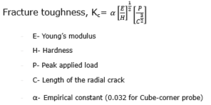
Ideal probe area function for a Berkovich probe: - C0 = 24.5
- C1-C5 = fitted parameters
2.Cube Corner: The 90 degree (cube corner) nanoindentation probes are similar to the Berkovich probes in that they are also 3-sided pyramidal probes . The total included angle of the cube corner probes is 90°. The half-angle, or the angle from the perpendicular to one face (angle θ), is 35.26°, which gives the cube corner probe an aspect ratio of 1:1. Because the aspect ratio is higher, it is much simpler to make the radius of curvature smaller. The primary advantage that the cube corner probe has over other probes is the sharpness. The radius of curvature can be less than 40 nm. This allows smaller indentations to be performed, while still creating plastic deformation.
Ideal probe area function for a cube corner probe:
- C0 = 2.598
- C1-C5 = fitted parameters
Typical indentation applications for cube corner probes:
- Ultra-thin coatings less than 100 nm thick
- Micro/nano-composites
- Fracture of samples
- Micro/nano structured materials
3.Cono-Spherical: Cono-spherical probes are cone shaped nanoindentation probes with spherical ends. The available cone angles are 60°, 90°, and 120°. With all but the sharpest probes on soft materials, only the spherical end of the probe will be in contact with the sample, so the cone angle is generally not as important.
Typical indentation applications for Cono-speherical probes:
- Sharper conical probes less than 1 µm are primarily used for scratch experiments
- Large radius probes are normally used to investigate very soft samples or for compression experiments.
Ideal probe area function for a Cono-spherical probe:
- C0 = -π or -3.14
- C1 = 2 × π × R or 6.28 × R, where R is the radii of the probe in nanometers
- C2-C5 = fitted parameters
The force modulation method offers a significant improvement in quasi-static Oliver-Pharr technique. In force modulation a small sinusoidal force (AC force) is superimposed on the quasi-static force (DC force) applied to the indenter. The resulting modulation in the displacement (AC displacement amplitude) and the phase shift between the AC force and displacement is measured using a lock-in amplifier. The contact stiffness is calculated from the amplitude and phase shift using a dynamic model. The advantage of force modulation is that the contact stiffness can be directly obtained continuously during indentation. Because the measurements are carried out at frequencies greater than 40Hz, it is less sensitive to thermal drift, allowing accurate observation of creep in nanoscale contacts. The technique can also be extended to study the viscoelastic properties of polymeric materials.
Hysitron’s powerful CMX algorithms lie at the core of nanoDMA III, is useful for measurements on thin films. CMX provides a quantitative and truly continuous measurement of mechanical properties—including hardness, storage modulus, loss modulus, complex modulus, and tan delta—as a function of indentation depth, frequency, and time. The challenge to study thin film/substrate system is explained:
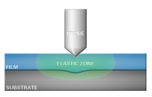
As this schematic illustrates, there is a zone of elastic strain underneath the indenter probe during an indentation test which extends well beyond the depth of the indent impression itself. As the indentation depth increases, the elastic zone grows, and at some point it begins to interact with the substrate, which influences the measurement. Results from displacements beyond a certain fraction of the film thickness become a mixture of the properties of the film and substrate. This extent of this convolution in properties, commonly referred to as “substrate effects,” depends not only on the indent depth, but also the indenter geometry and the modulus mismatch between film and substrate. CMX tests allow easy detection of substrate influence for thin film measurements.
Surface roughness is very important in Nanoindentation. Since the contact area is measured indirectly from depth of penetration, the natural roughness of real surfaces causes errors in the determination of the area of contact between the indenter and the specimen.
In general, surface roughness is characterized by the asperity height and the spatial distribution of them across the surface. Surface roughness can be quantified by a roughness parameter α where
α = σsR / a^2
σs is to first approximation, equal to the maximum asperity height, R is the indenter radius and a is the contact radius that would be obtained under the same load P for smooth surface. Note that α depends indirectly upon the load applied to the indenter. From the equation it can inferred that the surface roughness parameter increases with the increasing radius of indenter and increases with decreasing indenter load. Thus, for light loads with spherical indenters, surface roughness can be a significant effect. For sharper indenters, say Berkovich indenter with the tip radius of 100 nm , the effects of surface roughness are less severe.
To achieve repeatable data, as a rule of thumb and International standard ISO 14577-4, the average surface roughness Ra, should not be more than 5% of the depth at which mechanical properties are measured.